The global semiconductor industry is witnessing an unprecedented power struggle between two manufacturing giants: Taiwan Semiconductor Manufacturing Company (TSMC) and Samsung Electronics. Their competition extends beyond corporate rivalry—it’s reshaping global technology supply chains, influencing geopolitical strategies, and determining which innovations reach consumers. This comprehensive analysis examines how these foundry titans compare across critical dimensions including manufacturing technologies, market dominance, financial performance, and future roadmaps, particularly in the context of demand for chips and the evolving landscape of foundry services.
Executive Summary: The Strategic Importance of Semiconductor Dominance
In today’s technology-driven world, semiconductor manufacturing capability represents more than industrial capacity—it’s a cornerstone of economic and national security. TSMC and Samsung together control over 70% of the global foundry market, with their advanced nodes powering everything from smartphones to artificial intelligence systems. Their technological race has accelerated innovation while creating critical dependencies throughout the global technology ecosystem.
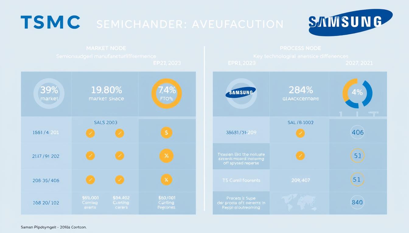
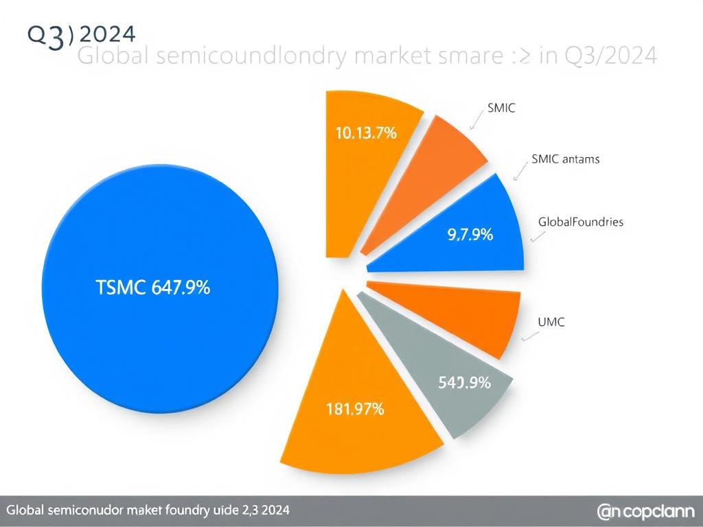
TSMC has established clear leadership in advanced process nodes, particularly at 5nm and 3nm, capturing nearly 65% of the global foundry market in 2024. The company’s pure-play foundry model has allowed it to focus exclusively on manufacturing excellence, building deep relationships with clients like Apple, Nvidia, and AMD. This specialization has translated into superior profit margins, reaching 56% gross profit margin compared to Samsung’s 38%.
Samsung, while trailing in foundry market share at approximately 12%, leverages its vertical integration across memory, logic, and consumer electronics. The company’s diversified approach provides resilience against market fluctuations but has resulted in lower foundry-specific profitability. Samsung’s aggressive investments in advanced nodes and packaging technologies signal its determination to narrow the gap with TSMC, particularly as AI and high-performance computing drive unprecedented demand for cutting-edge chips.
Company Histories and Milestones: Divergent Paths to Leadership
TSMC: The Pure-Play Pioneer
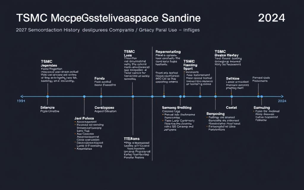
Founded in 1987 by Morris Chang, TSMC pioneered the pure-play foundry model, focusing exclusively on manufacturing chips designed by other companies. This specialization allowed TSMC to perfect its manufacturing processes without competing with its customers. Key milestones include:
- 1987: Established as the world’s first dedicated semiconductor foundry
- 2000: First foundry to offer copper interconnect technology
- 2011: First 28nm process technology
- 2015: First 16nm FinFET volume production
- 2020: First 5nm process node production
- 2022: Began 3nm production
- 2023: Announced Arizona fab expansion with $40 billion investment
Samsung: The Integrated Powerhouse
Samsung Electronics entered semiconductor manufacturing in 1974, initially focusing on memory chips before expanding into logic and foundry services. The company’s integrated approach spans design, manufacturing, and end products. Significant developments include:
- 1974: Began semiconductor business with memory chips
- 1992: Developed world’s first 64MB DRAM
- 2005: Launched foundry business
- 2016: Acquired Harman International to strengthen automotive electronics
- 2018: Began 7nm production
- 2022: First to announce 3nm Gate-All-Around (GAA) technology
- 2023: Announced $230 billion investment plan over 20 years
Manufacturing Technologies and Process Nodes: The Race to Atomic Scale
The competition between TSMC and Samsung is most visible in their race to develop increasingly advanced process nodes. As transistors approach atomic scale, each new node represents billions in R&D investment and years of development.
Current Process Node Comparison
| Process Node | TSMC | Samsung | Key Differences |
| 5nm | Mass production since 2020; N5, N5P variants; High yields (80%+) | 5LPE process; Lower yields (60-70%) | TSMC leads in power efficiency; Samsung offers competitive pricing |
| 4nm | N4, N4P variants; Used by Apple, AMD | 4LPE/4LPP; Used by Qualcomm | TSMC maintains yield advantage; Samsung improving density |
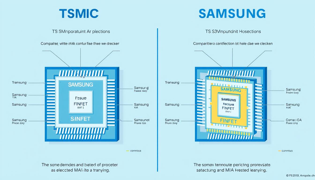
| 3nm | N3 in production since 2022; N3E in 2023; FinFET technology | First with 3nm GAA technology in 2022; MBCFET architecture | Samsung pioneered GAA; TSMC focused on yield stability |
| 2nm | Planned for 2025; Nanosheet technology | Planned for 2025; Second-gen GAA | Both transitioning to new transistor architectures |
“The difference between TSMC and Samsung isn’t just about process nodes—it’s about execution. TSMC consistently delivers what they promise, when they promise it, with the yields they promise. That reliability is worth a premium to customers designing multi-billion dollar chips.”
Beyond Nanometers: The New Metrics of Advancement
As traditional node naming becomes increasingly detached from physical dimensions, new metrics are emerging to compare process technologies:
Transistor Density
TSMC’s 3nm offers approximately 290 million transistors per square millimeter, while Samsung’s 3nm GAA technology delivers around 270 million. This density directly impacts chip performance and power efficiency.
Power Efficiency
TSMC’s 3nm process provides up to 30% power reduction compared to 5nm, while Samsung claims its 3nm GAA technology delivers up to 45% power savings—though real-world applications often show smaller differentials.
Yield Rates
TSMC maintains a significant advantage in production yields, particularly at new nodes. Industry estimates place TSMC’s 3nm yields at 60-70% in early production, compared to Samsung’s 20-30% for its 3nm GAA process.
Innovation and R&D Investments: Fueling the Next Generation
The semiconductor industry is among the most R&D-intensive sectors globally, with leading companies typically investing 15-20% of revenue in research and development. Both TSMC and Samsung have dramatically increased their R&D spending to maintain competitive positions.
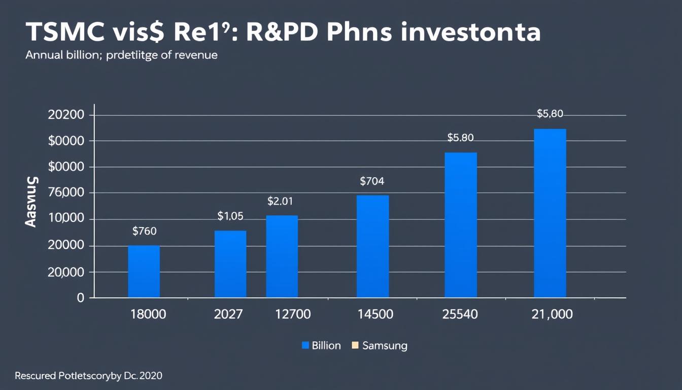
R&D Investment Comparison (2023-2024)
| Metric | TSMC | Samsung (Semiconductor Division) |
| 2023 R&D Spending | $7.1 billion | $9.8 billion |
| 2024 R&D Spending (Projected) | $8.5 billion | $11.2 billion |
| R&D as % of Revenue (2023) | 10.2% | 19.2% |
| 5-Year R&D Growth Rate | 87% | 63% |
| Patents Granted (2023) | 2,680 | 3,041 |
Key Innovation Focus Areas
TSMC’s Research Priorities
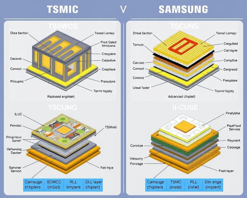
- Advanced Packaging: 3D fabric, System on Integrated Chips (SoIC), and CoWoS technologies
- New Transistor Architectures: Nanosheet FETs for 2nm and beyond
- Backside Power Delivery: Planned for A16 node in 2026/2027
- New Materials: Research into 2D materials and carbon nanotubes
- AI-Optimized Process Technologies: Specialized nodes for AI accelerators
Samsung’s Innovation Initiatives
- Gate-All-Around Technology: Multi-Bridge-Channel FET (MBCFET) architecture
- Heterogeneous Integration: I-Cube ETM and advanced chiplet technologies
- Custom HBM Memory: Configurable logic layer for memory-intensive applications
- Neuromorphic Computing: Brain-inspired computing architectures
- Quantum Computing: Long-term research into quantum processors
“While Samsung outspends TSMC on R&D in absolute terms, TSMC’s focused approach has yielded better returns on investment. Their research is tightly aligned with customer needs and manufacturing realities, whereas Samsung’s broader portfolio sometimes dilutes their focus.”
Client Base and Strategic Partnerships: The Customer Advantage
The client portfolios of TSMC and Samsung reveal significant differences in their market positioning and competitive strengths. TSMC has secured relationships with most leading fabless semiconductor companies, while Samsung leverages its internal chip needs alongside external customers.
| Client Category | TSMC Key Clients | Samsung Key Clients | Strategic Implications |
| Mobile SoCs | Apple, MediaTek, Qualcomm (partial) | Qualcomm (partial), Samsung LSI (internal) | Apple’s exclusive use of TSMC provides stable, high-volume production |
| AI/ML Processors | Nvidia, AMD, Google TPU | Tesla FSD chip, Samsung NPU (internal) | TSMC dominates high-performance AI accelerator market |
| CPUs/GPUs | AMD, Intel (partial), Apple | IBM, Intel (partial) | TSMC’s process advantage critical for compute-intensive applications |
| Automotive | NXP, Renesas, Mobileye | Tesla, Hyundai, Samsung Harman (internal) | Growing segment with Samsung leveraging vertical integration |
| IoT/Edge | Ambiq, Nordic, Silicon Labs | Samsung Electronics (internal), STMicroelectronics | TSMC’s specialty processes vs. Samsung’s integrated solutions |
Client Relationship Dynamics
TSMC’s Client Advantage
- Pure-play model eliminates competition with customers
- Consistent capacity allocation policies
- Proven track record of maintaining confidentiality
- Superior yield rates reduce client costs
- Extensive IP ecosystem and design support
Samsung’s Client Challenges
- Dual role as competitor and manufacturer creates conflicts
- Inconsistent capacity prioritization during shortages
- Lower yields increase client costs and risks
- Less mature design ecosystem
- Geographic concentration in South Korea
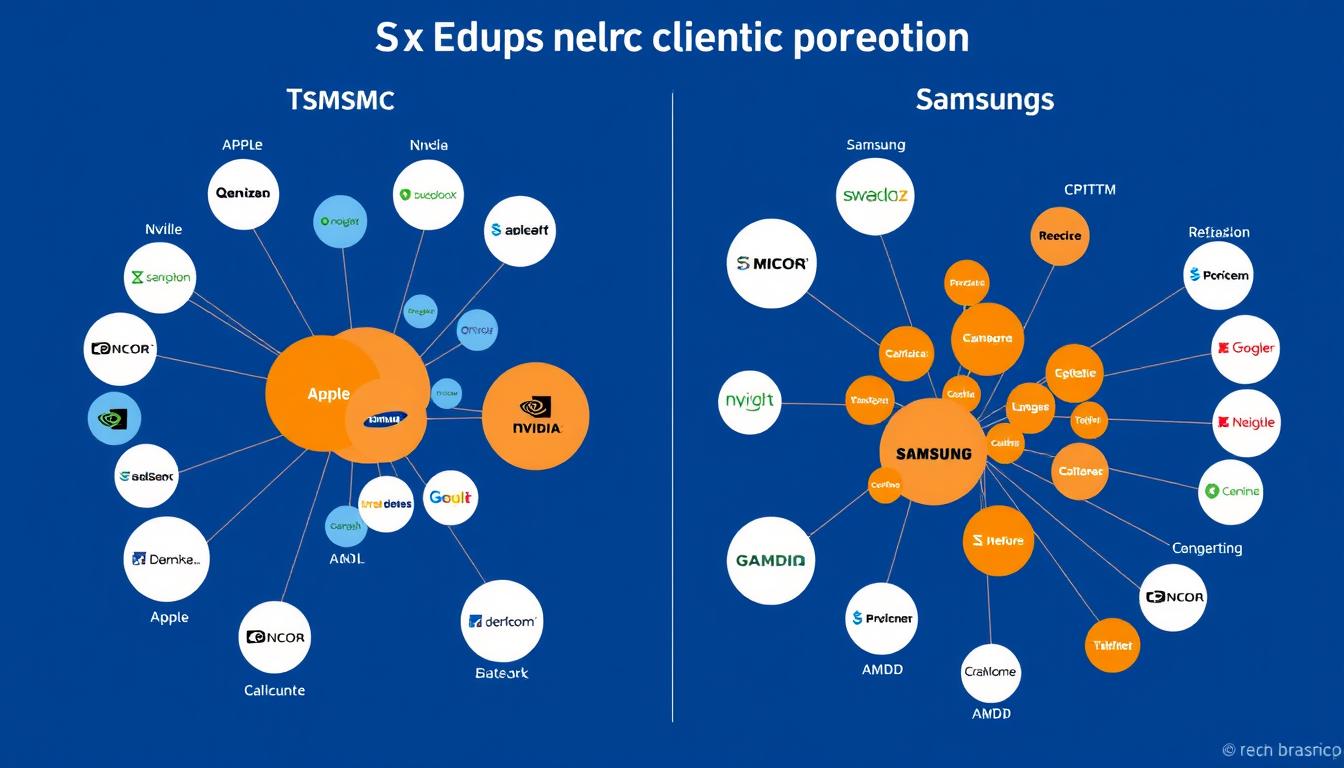
“The decision to partner with TSMC for our most advanced chips wasn’t just about technology—it was about trust. Their pure-play model means they’re never competing with us, and their track record of protecting IP is unmatched in the industry.”
Supply Chain and Geopolitical Considerations: Risk and Resilience
The semiconductor industry operates within an increasingly complex geopolitical landscape, with national security concerns, export controls, and regional tensions shaping strategic decisions. Both TSMC and Samsung face distinct challenges and opportunities in this environment.
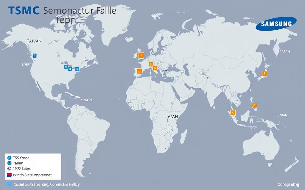
Geographic Concentration and Diversification Efforts
TSMC’s Taiwan Concentration
TSMC’s manufacturing capacity remains heavily concentrated in Taiwan, creating potential vulnerabilities:
- Over 90% of advanced node capacity (7nm and below) located in Taiwan
- Exposure to China-Taiwan tensions and natural disaster risks
- U.S. government pressure to diversify manufacturing locations
- $40 billion Arizona investment represents significant shift
- Japan and potential European facilities part of diversification strategy
Samsung’s Korean Base
Samsung’s semiconductor operations are primarily based in South Korea, with some diversification:
- Approximately 80% of capacity in South Korea (Hwaseong, Pyeongtaek, Giheung)
- Existing U.S. presence in Austin, Texas
- New $17 billion facility in Taylor, Texas under construction
- Proximity to North Korea presents geopolitical risk
- Less concentrated than TSMC but still regionally focused
Export Controls and Technology Restrictions
Government policies increasingly impact semiconductor manufacturing strategies, with U.S.-China tensions creating particular challenges:
| Policy Area | Impact on TSMC | Impact on Samsung |
| U.S. Export Controls | Restrictions on serving Chinese customers like HiSilicon; estimated 10-15% revenue impact | Less exposure to Chinese fabless customers; primarily affects memory sales |
| CHIPS Act Subsidies | Eligible for significant subsidies for Arizona fabs; estimated $5-7 billion | Eligible for Texas expansion subsidies; estimated $3-5 billion |
| Equipment Restrictions | Limited impact on non-Chinese operations; concerns about future escalation | Similar to TSMC; primarily affects Chinese memory operations |
| Talent Mobility | Challenges in staffing U.S. operations with experienced personnel | Established U.S. presence provides advantage in talent acquisition |
“The geopolitical dimension of semiconductor manufacturing has become as important as the technological one. Companies must now balance innovation with resilience, considering not just where they can manufacture most efficiently, but where they can do so most securely.”
Financial Performance and Growth Prospects: The Bottom Line
Financial metrics reveal significant differences in how TSMC and Samsung’s semiconductor businesses perform, reflecting their distinct business models and market positions.
Profitability Comparison (2024)
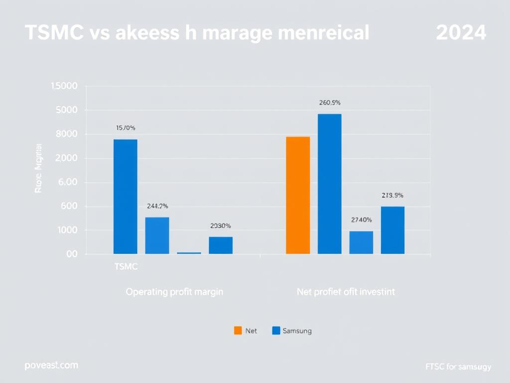
TSMC’s financial performance demonstrates the advantages of its focused business model, with superior margins across all key metrics. In 2024, TSMC achieved a gross profit margin of 56%, operating profit margin of 46%, and net profit margin of 41%—all significantly higher than Samsung’s semiconductor division.
Samsung’s semiconductor business, while generating higher absolute gross profit ($83.9 billion compared to TSMC’s $50.6 billion), achieved lower margins: 38% gross profit margin, 11% operating profit margin, and 12% net profit margin in 2024. This reflects both the competitive challenges in memory markets and the lower profitability of its foundry business relative to TSMC.
Revenue Growth and Market Outlook
TSMC’s Growth Trajectory
TSMC has demonstrated exceptional revenue growth, driven by advanced node adoption and expanding customer base:
- 2023 revenue: $69.3 billion (15.5% YoY growth)
- Q3 2024 revenue: $23.53 billion (13% QoQ growth)
- 5-year CAGR (2019-2024): 18.7%
- Projected 2025 revenue: $85-90 billion
- Key growth drivers: AI accelerators, HPC, advanced automotive
Samsung Semiconductor Outlook
Samsung’s semiconductor business has faced more volatility, particularly in memory markets:
- 2023 semiconductor revenue: $50.99 billion (22% YoY decline)
- Q3 2024 foundry revenue: Decreased 12.4% QoQ
- 5-year CAGR (2019-2024): 3.2%
- Projected 2025 semiconductor revenue: $60-65 billion
- Key growth drivers: Memory recovery, automotive, internal demand
“TSMC’s financial performance isn’t just about current technology leadership—it’s about consistent execution quarter after quarter, year after year. Their ability to translate technological advantages into financial results has been remarkable, and it gives them the resources to maintain their lead.”
Future Strategies and Roadmaps: The Path Forward
Both TSMC and Samsung have articulated ambitious plans for the future, focusing on advanced nodes, new transistor architectures, and innovative packaging technologies to address the growing demands of AI, high-performance computing, and other emerging applications.
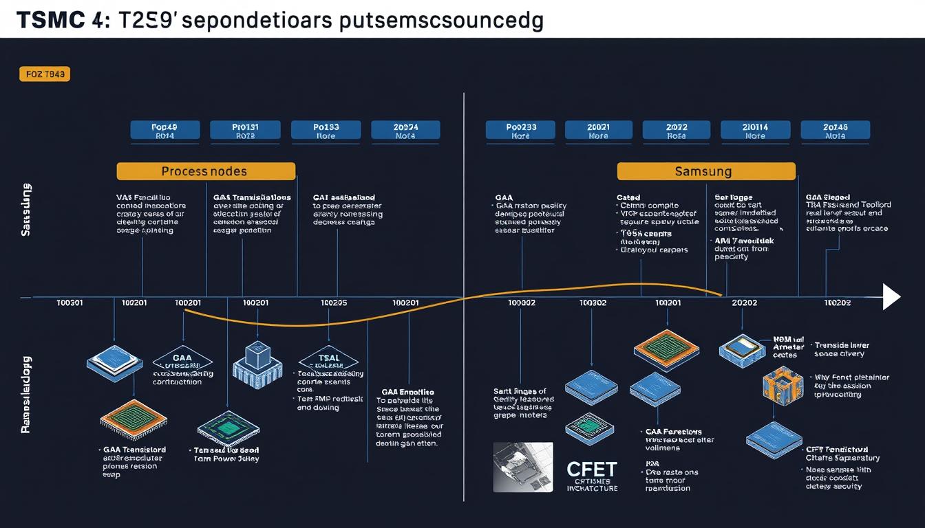
Process Technology Roadmaps
| Timeline | TSMC Milestones | Samsung Milestones |
| 2024-2025 | N3E enhanced 3nm node; N3P performance-optimized variant | SF3E enhanced 3nm GAA; SF3P performance variant |
| 2025-2026 | N2 (2nm) with nanosheet transistors; A16 development | SF2 (2nm) with second-gen GAA; SF2P performance variant |
| 2026-2027 | A16 (1.6nm) with backside power delivery; CFET research | SF1.4 (1.4nm) with backside power delivery; SF2Z with new materials |
| 2027-2029 | A14 (1.4nm) with new materials; potential CFET introduction | SF1.0 (1nm) with CFET architecture; new substrate materials |
Strategic Focus Areas
Advanced Packaging
Both companies are investing heavily in heterogeneous integration technologies:
- TSMC: CoWoS, InFO, SoIC with 3Dblox design language
- Samsung: I-Cube ETM, 3DCODE, logic-on-logic stacking
- Both: UCIe and BoW standards adoption
AI Optimization
Specialized technologies for AI workloads:
- TSMC: HPC-optimized process variants, high-bandwidth memory integration
- Samsung: Custom HBM with logic layer, neuromorphic computing research
- Both: Power delivery innovations for massive AI accelerators
Geographic Expansion
Diversification of manufacturing footprint:
- TSMC: Arizona, Japan, potential European facility
- Samsung: Texas expansion, potential facilities in Singapore, Vietnam
- Both: Balancing geopolitical risks with cost considerations
“The next frontier in semiconductor manufacturing isn’t just about smaller transistors—it’s about system-level integration. The winners will be those who can combine advanced nodes with innovative packaging to deliver complete solutions optimized for specific workloads, particularly AI.”
Challenges and Risks: The Road Ahead
Despite their dominant positions, both TSMC and Samsung face significant challenges that could impact their future competitiveness and market positions.
TSMC’s Key Challenges
Geopolitical Vulnerability
TSMC’s concentration in Taiwan creates significant risk given China-Taiwan tensions. While diversification efforts are underway, the majority of advanced capacity remains in Taiwan, creating potential supply chain vulnerabilities for global technology companies.
Cost Escalation
Each new process node requires exponentially higher investment. TSMC’s capital expenditure has grown from $14.9 billion in 2019 to over $30 billion in 2023. These rising costs must be passed to customers, potentially slowing adoption of the most advanced nodes.
Competitive Threats
Intel’s foundry ambitions, backed by significant government support, could challenge TSMC’s dominance in North America and Europe. Meanwhile, China’s SMIC continues to advance despite restrictions, potentially threatening TSMC’s position in certain market segments.
Samsung’s Key Challenges
Yield and Execution
Samsung has consistently struggled with yield rates at advanced nodes, particularly with its 3nm GAA technology. These challenges have undermined customer confidence and limited market share growth despite technological innovation.
Business Model Conflicts
Samsung’s dual role as both a foundry service provider and a competitor to potential customers creates inherent conflicts. This has limited its ability to attract certain high-profile clients, particularly in consumer electronics and mobile processors.
Memory Market Volatility
Samsung’s semiconductor business remains heavily exposed to memory markets, which experience more pronounced boom-bust cycles than logic. This volatility can impact overall financial performance and limit resources available for foundry investments during downturns.
Conclusion: The Future of Semiconductor Manufacturing
The competition between TSMC and Samsung will continue to shape the global semiconductor landscape for years to come. TSMC currently maintains clear leadership in the foundry business, with superior market share, profit margins, and customer relationships. Its focused business model and execution excellence have created significant advantages that will be difficult for competitors to overcome in the near term.
Samsung, despite trailing in foundry market share, brings considerable strengths through its vertical integration, memory leadership, and massive scale. Its aggressive investments in advanced nodes and packaging technologies demonstrate a long-term commitment to narrowing the gap with TSMC. The company’s diversified business model provides resilience but also creates challenges in competing with TSMC’s pure-play approach.
As the semiconductor industry enters an era of AI-driven demand and increasing geopolitical complexity, both companies will need to balance technological innovation with supply chain resilience. The winners will be those who can not only develop the most advanced manufacturing processes but also deploy them at scale while navigating an increasingly complex global landscape.
Who currently leads in semiconductor manufacturing technology?▶
TSMC currently maintains a lead in semiconductor manufacturing technology, particularly in terms of yield rates and production maturity at advanced nodes. While Samsung was first to announce 3nm production with GAA technology, TSMC’s 3nm FinFET process has demonstrated superior yield rates and performance in commercial products. Both companies are racing to develop 2nm technology, expected around 2025.
How does the TSMC vs Samsung semiconductor comparison affect consumers?▶
The TSMC vs Samsung semiconductor competition directly impacts consumers through the performance, efficiency, and availability of electronic products. Devices using TSMC-manufactured chips (like Apple iPhones) often demonstrate better performance and power efficiency, while Samsung’s vertical integration allows it to quickly bring innovations to its own consumer products. The competition drives innovation while affecting product pricing and features across the technology ecosystem.
What are the geopolitical implications of TSMC and Samsung’s dominance?▶
The concentration of advanced semiconductor manufacturing in Taiwan (TSMC) and South Korea (Samsung) creates significant geopolitical vulnerabilities in the global technology supply chain. This has prompted major initiatives like the U.S. CHIPS Act and similar programs in Europe and Japan to diversify manufacturing locations. Both companies are expanding globally, with major investments in the United States, though the majority of advanced capacity remains in their home regions.
